PCB Board Preparation
Figure showing steps involved in PCB board
preparation.

Step 1

Step 2

Step 3

Step 4

Step 5
For
printing of PCB design layouts to be done, first the plain PCB board of
matching size to the design layouts need to be prepared following the steps
shown in figure above.
Step
1 shows cutting of PCB design layouts from the printed OHP paper. In step 2,
the plain PCB board are being cut following the size of cut out design from OHP
sheet. Step 3 is about polishing the copper surface of plain PCB board to
remove the oxide layer, followed by wiping of oxide dust with tissue paper and
then with thinner as in step 4 and 5 respectively.
Ironing Method
Figure showing steps involved in printing PCB layout
designed onto PCB board prepared.

Step 1

Step 2

Step 3
After
preparing plain PCB board of matching size, printing of PCB design layouts on
plain PCB can now be done following steps shown in figure above. First, the
printed side of the OHP sheet need to be placed onto the copper surface of PCB
board. Then, with the board and OHP sheet placed under a piece of white paper,
the ironing can be done for printing process. Lastly, if the printing does not
seem to be perfect with some of the dark line not appearing, then a permanent
marker needs to be used to draw onto it.
Etching
Etching
is a process of removing unwanted copper part on the PCB board designed,
leaving only the copper part covered with permanent marker. To start etching
process, the final product after the printing process as shown in step 1 of
figure below need to be immersed in a container containing the etching acid
which is dark brown in colour, as in step 2 below. The container need to be
shaken gently and constantly for the acid to move around the surface of the
copper layer of the board for more effective and rapid etching process. After
etching the unwanted copper, now it can be clearly seen as in step 3 below that
only the permanent marker lines are left over. In step 3, the board was cleaned
with plain water to remove the acid layer.
Figure showing steps involved in etching process.

Step 1

Step 2

Step 3
Removing Marker Layer
Following
after the etching process are process of removing permanent marker layer
covering the copper layer. The permanent marker is removed using thinner by
wiping with sponge as in figure a below. The result is PCB board with shiny
copper design layout on top of it as in figure b below.
Figure showing process of removing permanent marker on
PCB layout.

a

b
Checking Connectivity
When
the multimeter touches connected copper lines, it gives reading of “0” as in
figure b below. If the copper lines are disconnected, it gives reading of “1”
as in figure a below.
Figure showing process of checking connectivity for
the PCB layout.

a

b
Drilling
Figure
showing PCB hand drill used in the project.

Figure
showing drilling process.

Step 1

Step 2
Drilling
of PCB need to be done carefully to ensure the PCB layouts are not damaged or
disconnected. For that, the hand drill had to be held firmly and be pointed to
the exact drilling point without shacking when started to drill as shown in
step 1. The drilled hole need to be checked and cleaned from the board dust
produced during drilling process as to prevent the drilled hole being blocked as
shown in step 2 figure.
Completion To Hardware Development
Figure showing PCB circuits board prepared for the
component placement and soldering.

Soldering
Figure showing soldering process after the component
placement.

a
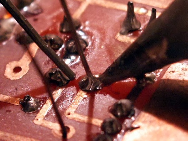
b
To
start soldering process, several tools and material have to be prepared first,
such as soldering iron, solder lead, solder paste, sucker, and wet cloth as
shown in figure a above. Before start soldering, the method need to be
understand first in order to produce good soldering work. When soldering, first
the copper pad surrounding the component leg need to be heated. Then, solder
lead need to be touched on to the heated pad and let it melt to stick to the
component leg perfectly as shown in figure b above.
No comments:
Post a Comment